
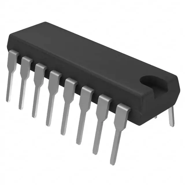
이미지는 참조용입니다.
74HC5555N,112
+BOMIC OSC TIMER W/OSC 89MHZ 16-DIP
-
제조업체은지포미국주식회사
-
제조업체 부품 #74HC5555N,112
-
데이터시트 74HC5555N,112 DataSheet
-
패키지 DIP-16
-
재고9738
365 1일 품질 보증
7*24 영업 시간 서비스 보증
90-판매 후 1일 보증
정품 보증
사양
| 속성 | 가치 |
| Supplier | NXP USA Inc. |
| Package / Case | Tube |
| Series | 74HC |
| Part Status | Obsolete |
| Type | Timer/Oscillator (Single) |
| Frequency | 89MHz |
| Voltage - Supply | 2V ~ 6V |
| Operating Temperature | -40°C ~ 125°C |
| Supplier Device Package | 16-DIP |
개요
Description
The chip operates at a wide voltage range, typically from 2V to 6V, making it versatile for various applications. It features low power consumption due to its CMOS technology, and it provides high noise immunity. The 74HC5555N,112 can count from 0 to 15 (in binary), with outputs that can be easily interfaced with other digital systems.
Key features include synchronous operation, where all bits change simultaneously with the clock pulse, and a master reset that sets the counter to zero. The IC is housed in a standard DIP package, allowing for easy implementation and prototyping in electronic projects.
Equivalent
Features
1. Wide Supply Voltage Range: It operates from 2V to 6V, which makes it compatible with both TTL and CMOS logic levels.
2. Low Power Consumption: Due to CMOS technology, it offers low power consumption, making it suitable for battery-operated devices.
3. Configurable Timing: It can be used in monostable or astable modes, allowing for diverse timing applications such as pulse generation, delay timers, and oscillators.
4. High-Speed Operation: It provides fast operation with typical propagation delays that are much better than older 555 timer versions.
5. Enhanced Temperature Range: It operates effectively over a wide temperature range, making it reliable in different environmental conditions.
These features make the 74HC5555N,112 versatile for use in electronic projects requiring precise timing control.
Pinout
1. Pin 1 (A0): Address input.
2. Pin 2 (A1): Address input.
3. Pin 3 (A2): Address input.
4. Pin 4 (A3): Address input.
5. Pin 5 (A4): Address input.
6. Pin 6 (A5): Address input.
7. Pin 7 (A6): Address input.
8. Pin 8 (GND): Ground.
9. Pin 9 (A7): Address input.
10. Pin 10 (OE): Output Enable, active low.
11. Pin 11 (Q7): Data output.
12. Pin 12 (Q6): Data output.
13. Pin 13 (Q5): Data output.
14. Pin 14 (Q4): Data output.
15. Pin 15 (VCC): Positive power supply.
16. Pin 16 (Q3): Data output.
The 74HC5555N is primarily used in memory addressing and data output applications, where it decodes address lines to provide data outputs.


