
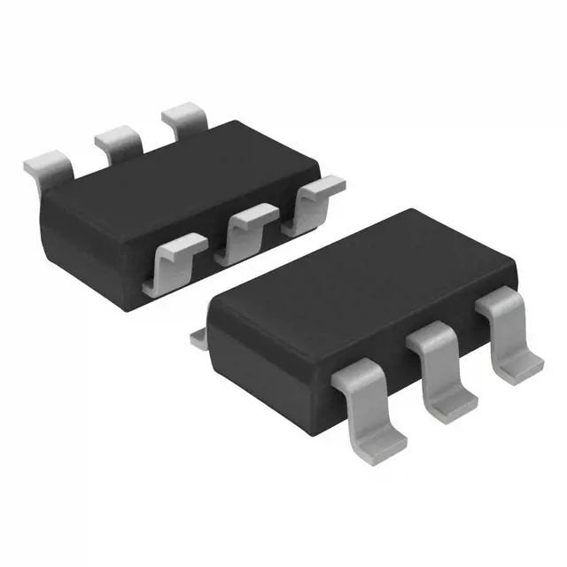
사양
| 속성 | 가치 |
| Package / Case | Tape & Reel (TR),Cut Tape (CT) |
| Part Status | Active |
| FET Type | N-Channel |
| Technology | MOSFET (Metal Oxide) |
| Drain to Source Voltage (Vdss) | 30 V |
| Current - Continuous Drain(Id) @ 25°C | 3.5A (Ta) |
| Drive Voltage(Max Rds On Min Rds On) | 4.5V, 10V |
| Rds On(Max) @ Id Vgs | 25mOhm @ 7A, 10V |
| Vgs(th)(Max) @ Id | 3V @ 250µA |
| Gate Charge(Qg)(Max) @ Vgs | 12 nC @ 10 V |
| Vgs(Max) | ±20V |
| Input Capacitance(Ciss)(Max) @ Vds | 560 pF @ 24 V |
| Power Dissipation (Max) | 500mW (Ta) |
| Operating Temperature | -55°C ~ 150°C (TJ) |
| Mounting Type | Surface Mount |
| Supplier Device Package | 6-TSOP |
개요
Description
NTGS4141NT1G is a small-signal N-channel MOSFET from ON Semiconductor, designed for low-voltage, high-speed switching applications. Key features include a low threshold voltage (typically 1V), fast switching speeds, and low on-resistance (RDS(on)), making it ideal for power management in portable electronics, load switching, and signal amplification.
It operates with a drain-source voltage (VDS) of 20V and a continuous drain current (ID) of 1.7A, housed in a compact SOT-23 package for space-constrained designs. The device is optimized for efficiency in battery-powered systems, such as smartphones, tablets, and IoT devices.
Advantages include minimal gate charge (Qg) for reduced switching losses and compatibility with low-voltage logic (1.8V–5V). Its RoHS compliance ensures environmental safety.
For detailed specifications, refer to the datasheet on ON Semiconductor’s website.
It operates with a drain-source voltage (VDS) of 20V and a continuous drain current (ID) of 1.7A, housed in a compact SOT-23 package for space-constrained designs. The device is optimized for efficiency in battery-powered systems, such as smartphones, tablets, and IoT devices.
Advantages include minimal gate charge (Qg) for reduced switching losses and compatibility with low-voltage logic (1.8V–5V). Its RoHS compliance ensures environmental safety.
For detailed specifications, refer to the datasheet on ON Semiconductor’s website.
Equivalent
Equivalent products to the NTGS4141NT1G (N-channel MOSFET by ON Semiconductor) include:
- DMN1019USN-7 (Diodes Incorporated)
- BSS138 (Infineon/NXP/others)
- 2N7002 (Various manufacturers)
These are small-signal MOSFETs with similar specs (30V, ~200mA, SOT-23 package). Verify parameters like threshold voltage and RDS(on) for exact compatibility.
- DMN1019USN-7 (Diodes Incorporated)
- BSS138 (Infineon/NXP/others)
- 2N7002 (Various manufacturers)
These are small-signal MOSFETs with similar specs (30V, ~200mA, SOT-23 package). Verify parameters like threshold voltage and RDS(on) for exact compatibility.
Features
The NTGS4141NT1G is a small-signal N-channel MOSFET with the following key features:
- Low Threshold Voltage (VGS(th)): ~0.5V (typ.), suitable for low-voltage applications.
- Low On-Resistance (RDS(on)): ~0.6Ω (max. at VGS=4.5V), ensuring efficient switching.
- Compact Package: SOT-23 (3-pin), ideal for space-constrained designs.
- Low Power Consumption: Designed for battery-operated devices.
- Fast Switching Speed: Enhances performance in high-frequency circuits.
- Low Gate Charge (Qg): Reduces drive power requirements.
Common applications include load switching, power management, and signal amplification in portable electronics.
- Low Threshold Voltage (VGS(th)): ~0.5V (typ.), suitable for low-voltage applications.
- Low On-Resistance (RDS(on)): ~0.6Ω (max. at VGS=4.5V), ensuring efficient switching.
- Compact Package: SOT-23 (3-pin), ideal for space-constrained designs.
- Low Power Consumption: Designed for battery-operated devices.
- Fast Switching Speed: Enhances performance in high-frequency circuits.
- Low Gate Charge (Qg): Reduces drive power requirements.
Common applications include load switching, power management, and signal amplification in portable electronics.
Pinout
The NTGS4141NT1G is a single N-channel MOSFET in a SOT-23-3 package, featuring 3 pins with the following functions:
1. Gate (G) – Controls the MOSFET's switching.
2. Drain (D) – Connects to the load (high-side terminal).
3. Source (S) – Connects to ground (low-side terminal).
Key specs:
- 30V drain-source voltage (VDS)
- 4A continuous drain current (ID)
- Low on-resistance (RDS(on)) for efficient switching.
Commonly used in power management, load switching, and DC-DC converters.
1. Gate (G) – Controls the MOSFET's switching.
2. Drain (D) – Connects to the load (high-side terminal).
3. Source (S) – Connects to ground (low-side terminal).
Key specs:
- 30V drain-source voltage (VDS)
- 4A continuous drain current (ID)
- Low on-resistance (RDS(on)) for efficient switching.
Commonly used in power management, load switching, and DC-DC converters.
Manufacturer
The NTGS4141NT1G is manufactured by ON Semiconductor, a leading global supplier of semiconductor-based solutions.
ON Semiconductor specializes in energy-efficient technologies, offering a wide range of products, including power management, analog, and discrete semiconductors for automotive, industrial, and consumer markets. The company is known for innovation in power efficiency and reliability.
The NTGS4141NT1G is a small-signal N-channel MOSFET, commonly used in switching and amplification applications. ON Semiconductor's components are widely trusted in electronics design.
ON Semiconductor specializes in energy-efficient technologies, offering a wide range of products, including power management, analog, and discrete semiconductors for automotive, industrial, and consumer markets. The company is known for innovation in power efficiency and reliability.
The NTGS4141NT1G is a small-signal N-channel MOSFET, commonly used in switching and amplification applications. ON Semiconductor's components are widely trusted in electronics design.
Application
The NTGS4141NT1G is a small-signal N-channel MOSFET commonly used in:
1. Load Switching – Efficient power management in portable devices.
2. Signal Amplification – Low-voltage applications in audio and RF circuits.
3. Battery Protection – Prevents reverse current in power systems.
4. Level Shifting – Interface conversion in logic circuits.
5. Consumer Electronics – Used in smartphones, tablets, and wearables due to its compact size and low power consumption.
Its key features include low threshold voltage, fast switching, and a small SOT-23 package, making it ideal for space-constrained designs.
1. Load Switching – Efficient power management in portable devices.
2. Signal Amplification – Low-voltage applications in audio and RF circuits.
3. Battery Protection – Prevents reverse current in power systems.
4. Level Shifting – Interface conversion in logic circuits.
5. Consumer Electronics – Used in smartphones, tablets, and wearables due to its compact size and low power consumption.
Its key features include low threshold voltage, fast switching, and a small SOT-23 package, making it ideal for space-constrained designs.
Package
The NTGS4141NT1G is a small-signal N-channel MOSFET available in a SOT-23 surface-mount package. This compact 3-pin package is widely used for space-constrained applications, offering reliable performance in switching and amplification circuits. The SOT-23 package dimensions are approximately 2.9mm x 1.3mm x 0.95mm.




